- 您现在的位置:买卖IC网 > Sheet目录3832 > PIC18F2520-I/ML (Microchip Technology)IC PIC MCU FLASH 16KX16 28QFN
PIC16(L)F1782/3
DS41579C-page 386
Preliminary
2011-2012 Microchip Technology Inc.
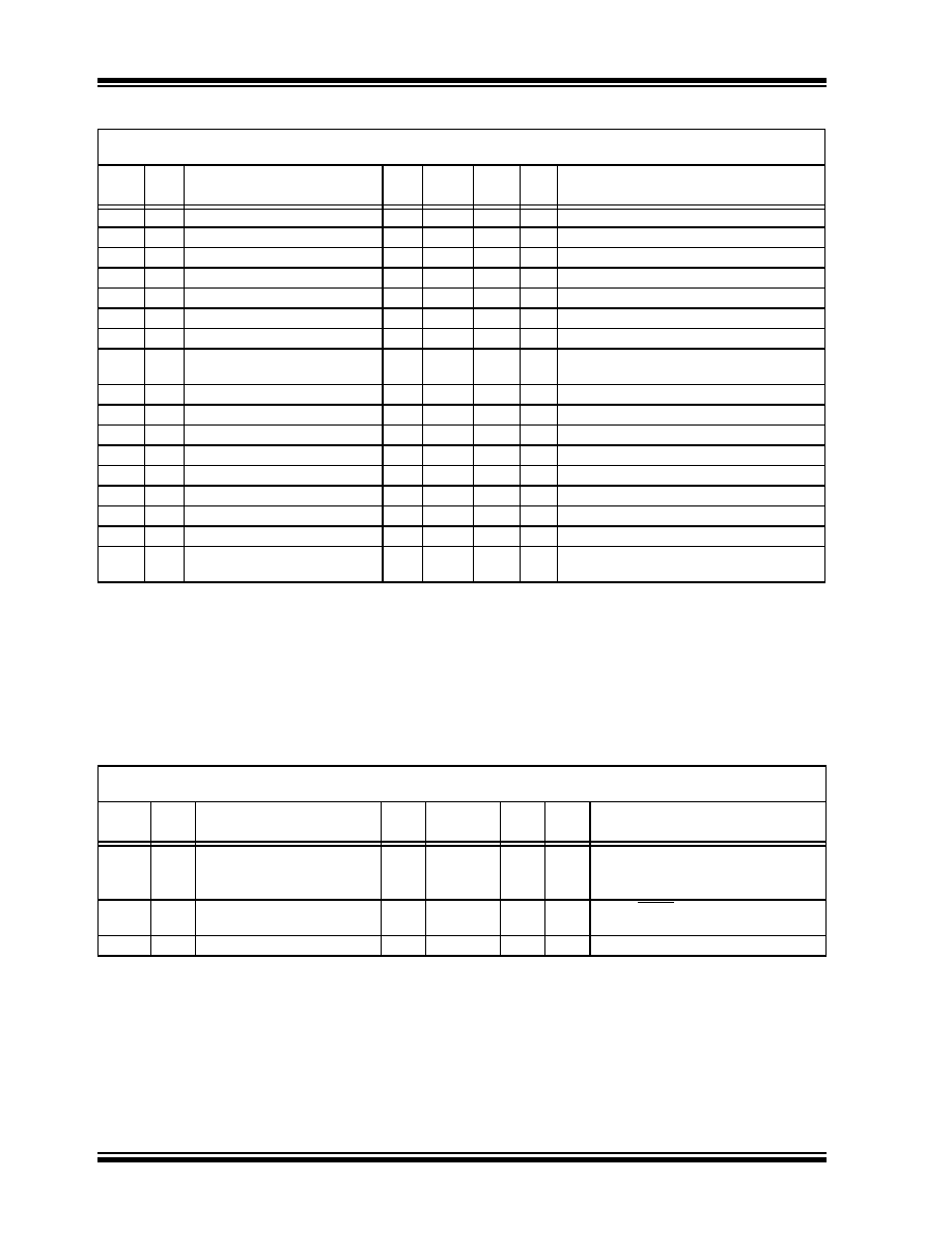
TABLE 30-8:
PIC16(L)F1782/3 A/D CONVERTER (ADC) 12-BIT DIFFERENTIAL CHARACTERISTICS:
TABLE 30-9:
PIC16(L)F1782/3 A/D CONVERSION REQUIREMENTS
Operating Conditions
VDD = 3V, Temp. = 25°C, Single-ended 2
s TAD, VREF+ = 3V, VREF- = VSS
Param
No.
Sym.
Characteristic
Min.
Typ
Max. Units
Conditions
AD01
NR
Resolution
—
10
bit
AD02
EIL
Integral Error
—
±1
±1.6
LSb
AD03
EDL
Differential Error
—
±1
±1.4
LSb No missing codes
AD04
EOFF Offset Error
—
±1
±2
LSb
AD05
EGN
Gain Error
—
±1
±2
LSb
AD06
VREF Reference Voltage(3)
1.8
—
VDD
VVREF = (VREF+ minus VREF-) (Note 5)
AD07
VAIN
Full-Scale Range
—
VREF
V
AD08
ZAIN
Recommended Impedance of
Analog Voltage Source
——
10
k
Can go higher if external 0.01F capacitor is
present on input pin.
AD09
NR
Resolution
—
12
bit
AD10
EIL
Integral Error
—
±2
—
LSb
AD11
EDL
Differential Error
—
±2
—
LSb
AD12
EOFF Offset Error
—
±1
—
LSb
AD13
EGN
Gain Error
—
±1
—
LSb
AD14
VREF Reference Voltage(3)
1.8
—
VDD
VVREF = (VREF+ minus VREF-) (Note 5)
AD15
VAIN
Full-Scale Range
—
VREF
V
AD16
ZAIN
Recommended Impedance of
Analog Voltage Source
——
10
k
Can go higher if external 0.01F capacitor is
present on input pin.
*
These parameters are characterized but not tested.
Data in “Typ” column is at 3.0V, 25°C unless otherwise stated. These parameters are for design guidance only and are not
tested.
Note 1: Total Absolute Error includes integral, differential, offset and gain errors.
2: The A/D conversion result never decreases with an increase in the input voltage and has no missing codes.
3: ADC VREF is from external VREF, VDD pin or FVR, whichever is selected as reference input.
4: When ADC is off, it will not consume any current other than leakage current. The power-down current specification
includes any such leakage from the ADC module.
5: FVR voltage selected must be 2.048V or 4.096V.
Standard Operating Conditions (unless otherwise stated)
Operating temperature
-40°C
TA +125°C
Param
No.
Sym.
Characteristic
Min.
Typ
Max.
Units
Conditions
AD130* TAD
A/D Clock Period
1.0
—
9.0
sTOSC-based
A/D Internal RC Oscillator
Period
1.0
1.6
6.0
s
ADCS<1:0> = 11 (ADRC mode)
AD131
TCNV
Conversion Time (not including
Acquisition Time)(1)
—15—
TAD
Set GO/DONE bit to conversion
complete
AD132* TACQ
Acquisition Time
—
5.0
—
s
*
These parameters are characterized but not tested.
Data in “Typ” column is at 3.0V, 25°C unless otherwise stated. These parameters are for design guidance only and are not
tested.
Note 1: The ADRES register may be read on the following TCY cycle.
发布紧急采购,3分钟左右您将得到回复。
相关PDF资料
AT87C51RC2-SLSUL
IC 8051 MCU 32K OTP 30MHZ 44PLCC
AT87C51RC2-RLTUM
IC 8051 MCU 32K OTP 40MHZ 44VQFP
AT87C51RC2-RLTUL
IC 8051 MCU 32K OTP 30MHZ 44VQFP
213684-4
34 PLUG KIT,M-SER,CC,JS,W/HOOD
202515-3
CONN PLUG BLOCK 42POS BLUE
202515-2
CONN PLUG M-SERIES 42POS
AT87C51RB2-RLTUL
IC 8051 MCU 16K OTP 30MHZ 44VQFP
AT87C51RB2-3CSUM
IC 8051 MCU 16K OTP 40MHZ 40DIP
相关代理商/技术参数
PIC18F2520-I/ML
制造商:Microchip Technology Inc 功能描述:8-Bit Microcontroller IC
PIC18F2520-I/SO
功能描述:8位微控制器 -MCU 32KB 1536 RAM 25I/0 RoHS:否 制造商:Silicon Labs 核心:8051 处理器系列:C8051F39x 数据总线宽度:8 bit 最大时钟频率:50 MHz 程序存储器大小:16 KB 数据 RAM 大小:1 KB 片上 ADC:Yes 工作电源电压:1.8 V to 3.6 V 工作温度范围:- 40 C to + 105 C 封装 / 箱体:QFN-20 安装风格:SMD/SMT
PIC18F2520-I/SP
功能描述:8位微控制器 -MCU 32KB 3968 RAM 25I/O RoHS:否 制造商:Silicon Labs 核心:8051 处理器系列:C8051F39x 数据总线宽度:8 bit 最大时钟频率:50 MHz 程序存储器大小:16 KB 数据 RAM 大小:1 KB 片上 ADC:Yes 工作电源电压:1.8 V to 3.6 V 工作温度范围:- 40 C to + 105 C 封装 / 箱体:QFN-20 安装风格:SMD/SMT
PIC18F2520T-E/SO
功能描述:8位微控制器 -MCU 32KB Flash 1536RAM 23I/O RoHS:否 制造商:Silicon Labs 核心:8051 处理器系列:C8051F39x 数据总线宽度:8 bit 最大时钟频率:50 MHz 程序存储器大小:16 KB 数据 RAM 大小:1 KB 片上 ADC:Yes 工作电源电压:1.8 V to 3.6 V 工作温度范围:- 40 C to + 105 C 封装 / 箱体:QFN-20 安装风格:SMD/SMT
PIC18F2520T-I/ML
功能描述:8位微控制器 -MCU 32KB 3968 RAM 25I/O RoHS:否 制造商:Silicon Labs 核心:8051 处理器系列:C8051F39x 数据总线宽度:8 bit 最大时钟频率:50 MHz 程序存储器大小:16 KB 数据 RAM 大小:1 KB 片上 ADC:Yes 工作电源电压:1.8 V to 3.6 V 工作温度范围:- 40 C to + 105 C 封装 / 箱体:QFN-20 安装风格:SMD/SMT
PIC18F2520T-I/SO
功能描述:8位微控制器 -MCU 32KB 3968 RAM 25I/O RoHS:否 制造商:Silicon Labs 核心:8051 处理器系列:C8051F39x 数据总线宽度:8 bit 最大时钟频率:50 MHz 程序存储器大小:16 KB 数据 RAM 大小:1 KB 片上 ADC:Yes 工作电源电压:1.8 V to 3.6 V 工作温度范围:- 40 C to + 105 C 封装 / 箱体:QFN-20 安装风格:SMD/SMT
PIC18F2523-E/ML
功能描述:8位微控制器 -MCU 32KB FL 1536bytes- RAM 25I/O RoHS:否 制造商:Silicon Labs 核心:8051 处理器系列:C8051F39x 数据总线宽度:8 bit 最大时钟频率:50 MHz 程序存储器大小:16 KB 数据 RAM 大小:1 KB 片上 ADC:Yes 工作电源电压:1.8 V to 3.6 V 工作温度范围:- 40 C to + 105 C 封装 / 箱体:QFN-20 安装风格:SMD/SMT
PIC18F2523-E/SO
功能描述:8位微控制器 -MCU 32KB FL 1536bytes- RAM 25I/O RoHS:否 制造商:Silicon Labs 核心:8051 处理器系列:C8051F39x 数据总线宽度:8 bit 最大时钟频率:50 MHz 程序存储器大小:16 KB 数据 RAM 大小:1 KB 片上 ADC:Yes 工作电源电压:1.8 V to 3.6 V 工作温度范围:- 40 C to + 105 C 封装 / 箱体:QFN-20 安装风格:SMD/SMT